
For over a decade, the facility has supported short-term R&D for public and industrial projects, delivering breakthroughs in PID degradation analysis, contact deterioration, defect diagnostics in single/tandem cells, and module soiling. CSP-Nano offers detailed defect diagnostics via scientific instrumentation and trained-staff supervision on a daily-to-weekly basis, including fully inert sample handling and transfer. Available instruments include: ToF-SIMS with in-situ biasing and heating/cooling (2D/3D profiling, <100 nm resolution, ~10¹⁶–10¹⁷ at/cm³ detection limits); lab-based XPS/UPS combined with REELS and Raman spectroscopy (~10 µm lateral, <0.1 eV energy resolution, optional biasing); SEM with EDX mapping and EBIC/EBAC capability; and analytical (S)TEM offering sub-nm resolution for nanostructure and chemical analysis via EDX/EELS. These techniques have previously characterized perovskite (tandem) solar cells and contacts, with imaging-microstructure synergy uniquely enabling inhomogeneity assessment and root-cause diagnostics. Access is on-site, typically a four-week stay, with operator collaboration and full support in data analysis afterward.
Advanced Characterization
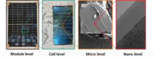
- Sample Preparation & Nano structural Analytics
- UHV operando-PES (coupled XPS/UPS/REELS/Raman) Operando-ToF-SIMS (electrical bias)
- SEM-EBIC
- (S)TEM-EDX/EELS